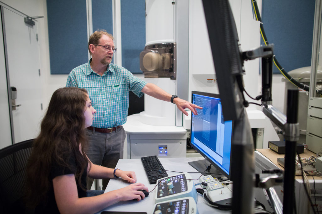


Our research utilizes the Nanoscale Characterization Facility at the Singh Center for Nanotechnology at the University of Pennsylvania — a shared, open-access microscopy suite available to Penn researchers, external academic users, and industry.
We utilize User facilities at the Singh Center for Nanotechnology and the Laboratory for Research on the Structure of Matter at Penn.
The scanning / transmission electron microscopes at the Singh Center also serve as the North American Demo site for the JEOL USA Corporation. We are grateful for their ongoing cooperation and collaboration, and for the day-to-day support of Dr. Douglas Yates and Dr. Jamie Ford.
Nanoscale Characterization Facility — home to our electron microscopes and FIB/SEM tools.
Supported by the National Nanotechnology Coordinated Infrastructure (NNCI) network (NNCI-1542153).
Laboratory for Research on the Structure of Matter & the Penn Materials Research Science and Engineering Center (DMR-1720530).
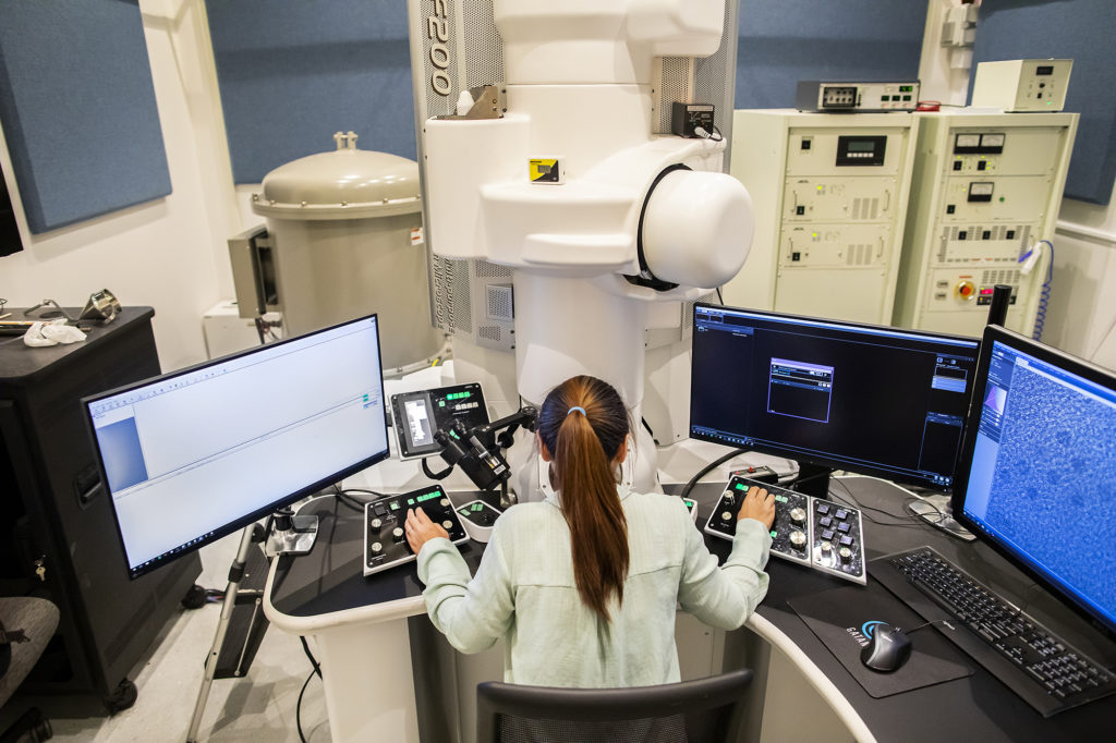
A scanning / transmission electron microscope with a spherical-aberration corrector on the probe-forming optics. The corrector optimizes 5th-order aberrations with improved stability, delivering an as-installed resolution of <0.63 Å at 200 kV and <1.92 Å at 30 kV.
Two large-area EDS spectrometers enable rapid atomic-resolution elemental mapping. A Gatan Image Filter with DualEELS provides accurate energy calibration, and a K2-IS direct electron detector (DQE ≈ 1.0) at the end of the filter enables ultra-sensitive detection at very high energy loss. The detector supports 2k × 2k acquisitions at 400 fps and 512 × 2k acquisitions at 1600 fps — ideal for in-situ and operando experiments. This was the first NEOARM installed in the U.S.
A 200 kV scanning / transmission electron microscope built for speed and flexibility — this is where we run most of our in-situ and operando experiments. Switching between TEM, STEM, diffraction, and spectroscopy modes is quick, which matters when a reaction won't wait.
A cold field-emission source, two large-area EDS spectrometers, and a Gatan OneView IS camera (30 fps for time-resolved imaging) together with STEMx capability make it well-suited to following dynamics in real time.
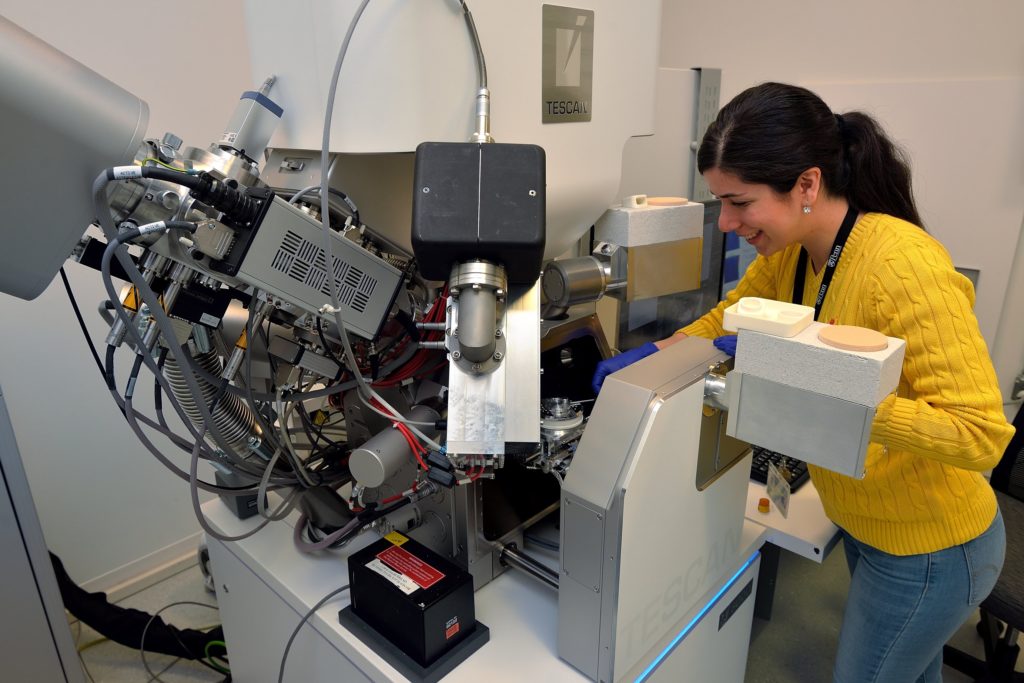
A versatile platform combining a plasma-source focused ion beam microscope with a high-resolution BrightBeam scanning electron microscope. The Xe⁺ plasma source generates focused beams up to 1 μA — milling rates up to 50× faster than prior Ga⁺ technology, without the deleterious ion-implantation artifacts that Ga⁺ leaves behind.
The BrightBeam SEM is field-free and ultra-high-resolution, with optics that preserve resolution at low accelerating voltages for non-conducting samples. Analytical modules include a Time-of-Flight Secondary Ion Mass Spectrometer (ToF-SIMS) — exceptional for light elements including H / D discrimination — an EDS spectrometer, a cryogenic stage (down to −160 °C) with a frozen-sample loadlock, and a cryogenic Kleindiek nanomanipulator for in-situ manipulation and frozen-section lift-out for TEM.
The microscopes are available to Penn researchers and external academic and industry users through the Singh Center. New users are trained by facility staff; the group is happy to discuss measurement strategy for specific scientific questions.